
Applied methods of power supply and galvanic isolation of gate drivers of power transistors in bridging end stages of Class D amplifiers and inverters
DOI:
https://doi.org/10.5604/01.3001.0012.1413Keywords:
Bootstrap power supply, charge pump, gate drivers, galvanic isolation of the control signals, Class-D amplifier, PWM, PSCPWM, DC-DC convertersAbstract
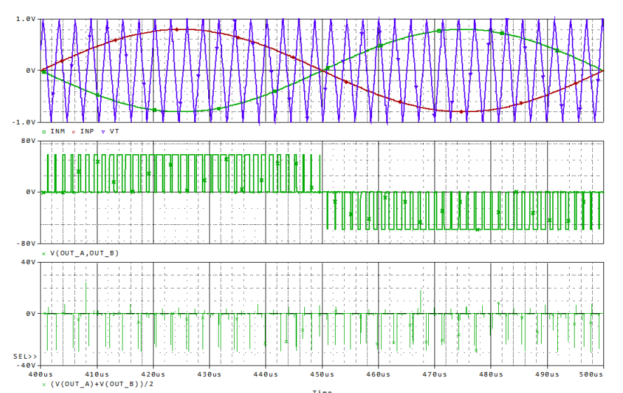
Various methods used for a floating high-side gate drive power supply and galvanic isolation of the Class-D amplifiers and different DC-AC or DC-DC converters have been reviewed and evaluated in the paper. On the basis of the literature, the bootstrap floating supply and self-boost charge pump topology for a gate drive high-side power supply, as well as control signal isolated systems with optically-isolated signals or with capacitive signal isolation have been described and compared. New topologies of the Class-BD amplifiers with Common-Mode (CM) free outputs using PSC PWM - Phase Shifted Carrier Pulse Width presented in the paper, shows that almost all gate drivers of the output stage transistors require floating power supply and galvanic isolation of the control signals. In the case of such circuits with multi-level PWM output, the most reliable and robust method for the floating gate drive power supply and galvanic isolation is self-boost charge pump topology with capacitive control signal isolation. Correct operation of the output stage of the proposed Class-BD amplifiers as well as the PWM modulator and self-boost charge pump topologies with capacitive control signal isolation have been verified using intensive Pspice simulation.
Downloads
References
Jasielski J, Kuta S, Machowski W. Class-BD Audio Amplifiers with Common-Mode Free Output, Mixed Design of Integrated Circuits & Systems (MIXDES), 2016 Proceedings of the 22st International Conference, Date 23-25 June 2016. Google Scholar
Jasielski J, Kołodziejski W, Kuta S. Cancellation of Common-Mode Output Signal in Class-BD Audio Amplifiers”, 2016 International Conference on Signals And Electronic Systems (ICSES), September 5-7, 2016, Kraków. Google Scholar
Berkhout M, Dooper L. Class-D Audio Amplifiers in Mobile Applications. IEEE Transactions On Circuits And Systems-I: Regular Papers, 2010, 57, 991-1002. Google Scholar
Morrison Ch, Weiss S, Macleod M, Stewart R. Comparison of Single- and Double-Sided Pulse Width Modulated Signalswith Non-Linear Predistortion, Proceedings of the 5th European DSP Education and Research Conference, 2012, Amsterdam. Google Scholar
Johansen M, Nielsen K. A Review and Comparison of Digital PWM Methods for Digital Pulse Modulation Systems, 107th AES Convention, 1999 September 24-27 New York. Google Scholar
Chung SK, Lim JG. Design of Bootstrap Power Supply for Half-Bridge Circuits using Snubber Energy Regeneration, Journal of Power Electronics, 2007, 7, 294-300. Google Scholar
Design and Application Guide of Bootstrap Circuit for High-Voltage Gate-Drive IC, AN-6076, 2008, Fairchild Semiconductor Corporation, Rev. 1.0.0 • 9/30/08. Google Scholar
Design Guide for Selection of Bootstrap Components, AN9052, 2008 Fairchild Semiconductor Corporation, Rev. 1.0.0 • 11/10/08. Google Scholar
Khoo GFW, Carter DRH, McMahon RA. Analysis of a chargé pump power supply with a floating voltage reference, IEEE Trans. Circuits Syst., 2000, 47, 1494–1501. Google Scholar
Meyer P., Tucker J., Providing Continuous Gate Drive Using a Charge Pump, 2011, Texas Instruments Incorporated, SLVA444–February 2011. Google Scholar
Lin RL, Lee FC. Single-power-supply-based transformerless IGBT/MOSFET gate driver with 100% high-side turn-on duty cycle operation performance using auxiliary bootstrapped charge pumper, Proc. IEEE Power Electronics Specialties Conf. (PESC), 1997, 1205–1209. Google Scholar
Park S, Jahns TM. A Self-Boost Charge Pump Topology for a Gate Drive High-Side Power Supply, IEEE Transactions on Power Electronics, 2005, 20, 300-307. Google Scholar
FODM8071 3.3V/5V Logic Gate Output Optocoupler with High Noise Immunity, www.fairchildsemi.com. Google Scholar
ISO7420x Low-Power Dual-Channel Digital Isolators, SLLS984I –JUNE 2009–REVISED JULY 2015, Texas Instruments, www.ti.com. Google Scholar
5-A and 5-A, 35-VMAX VDD FET and IGBT Single-Gate Driver, SLUSBA7D – DECEMBER 2012–REVISED APRIL 2013, www.ti.com. Google Scholar
Downloads
Published
How to Cite
Issue
Section
License
Copyright (c) 2018 University of Applied Sciences in Tarnow, Poland & Authors

This work is licensed under a Creative Commons Attribution-NonCommercial 4.0 International License.